
Sapphire (Al₂O₃) is far more than a gemstone. It is a foundational material in modern optoelectronics and semiconductor manufacturing. Owing to its outstanding optical transparency, thermal stability, chemical resistance, and mechanical hardness, sapphire has become a preferred substrate for GaN-based LEDs, Micro-LED displays, laser diodes, and other advanced electronic and photonic devices. A closer look at how sapphire substrates are grown, processed, and applied reveals why they remain indispensable to next-generation technologies.
1. Crystal Growth: The Basis of Sapphire Substrate Quality
The performance of a sapphire substrate begins with the quality of its single crystal. In industrial production, several crystal growth methods are used, each optimized for specific requirements related to crystal size, structural quality, and end-use applications.
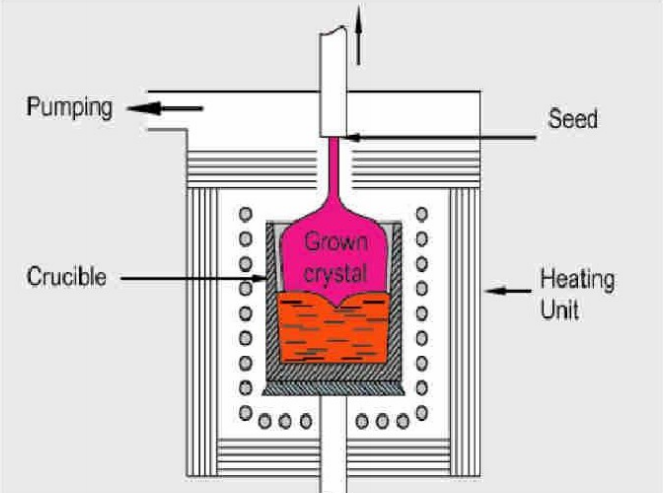
Kyropoulos (KY) Method
- Produces large-diameter sapphire crystals with relatively low internal stress
- Delivers excellent uniformity and high optical clarity
- Suitable for wafer production up to 12 inches in diameter
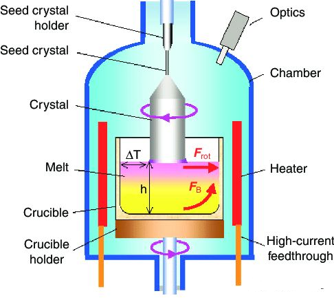
Czochralski (CZ) Method
- Involves pulling the crystal from molten sapphire while rotating it to control geometry
- Offers stable growth conditions, though internal stress is typically higher than in KY-grown crystals
- Commonly used for smaller-diameter wafers and cost-sensitive applications
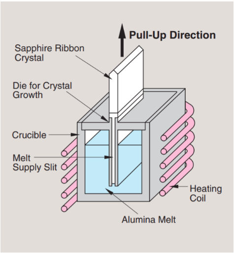
Edge-Defined Film-Fed Growth (EFG) Method
- Enables direct growth of shaped sapphire forms such as ribbons and tubes
- Supports complex or non-circular geometries for specialized optoelectronic components
- Widely used in LED windows and optical substrate applications
Each growth method influences critical parameters such as defect density, lattice uniformity, residual stress, and transparency, all of which ultimately affect downstream device yield and performance.
2. Precision Processing: From Ingot to Device-Ready Substrate
Once the sapphire crystal has been grown, the ingot undergoes a series of highly controlled processing steps to transform it into a substrate suitable for device fabrication.
Orientation and Coring
Crystallographic orientation is determined using X-ray diffraction or optical inspection methods. Common orientations include C-plane (0001), A-plane (11-20), and R-plane (1-102). The selected orientation has a direct impact on epitaxial growth behavior, optical performance, and mechanical characteristics.
Wafer Slicing
Diamond wire sawing is typically used to slice the ingot into wafers while minimizing subsurface damage. Key quality metrics at this stage include Total Thickness Variation (TTV), bow, and warp.
Double-Side Grinding and Chamfering
Double-side grinding ensures thickness uniformity, while edge chamfering strengthens wafer edges and reduces the risk of chipping or cracking during subsequent handling and processing.
Chemical Mechanical Polishing (CMP)
CMP is one of the most critical stages in substrate preparation. It reduces surface roughness to extremely low levels, often below Ra < 0.2 nm, and removes micro-scratches and residual damage. The result is an ultra-flat, defect-minimized surface essential for high-quality GaN epitaxy.
Cleaning and Contamination Control
Multi-stage chemical cleaning combined with ultra-pure water rinsing is used to eliminate particles, organic residues, and metallic contaminants, ensuring the substrate surface meets the stringent cleanliness requirements of high-performance device manufacturing.
3. Core Material Advantages of Sapphire Substrates
High-quality sapphire substrates offer a unique combination of properties that make them highly valuable in advanced manufacturing:
- Mechanical durability: With a Mohs hardness of 9, sapphire provides exceptional scratch and wear resistance
- Optical transparency: It exhibits high transmittance across ultraviolet, visible, and near-infrared wavelengths
- Thermal and chemical stability: Sapphire can withstand high-temperature epitaxial growth and aggressive chemical environments
- Epitaxial compatibility: Although sapphire has lattice mismatch with GaN, mature techniques such as ELOG help mitigate dislocation density and enable reliable epitaxial growth
4. Application Ecosystem
LEDs
C-plane sapphire remains the dominant substrate for GaN-based LED manufacturing. Patterned Sapphire Substrates (PSS) further enhance light extraction efficiency while also improving epitaxial layer quality.
Micro-LED Displays
Micro-LED technologies used in AR/VR systems, automotive head-up displays, and wearable devices rely on sapphire substrates for processes such as laser lift-off, high-density chip transfer, and precision alignment.
Laser Diodes and High-Performance Electronics
Sapphire serves as a stable platform for GaN-based laser diodes and provides mechanical support and thermal stability for advanced GaN and SiC power device structures.
Optical Windows and Protective Components
Because of its excellent UV and IR transmission as well as its superior hardness, sapphire is widely used in optical windows, sensor covers, camera protection, and high-pressure observation ports.
Precision Industrial and Medical Components
Beyond semiconductors, sapphire is also used in high-wear industrial and medical applications, including valves, surgical instruments, and precision mechanical components.
5. Future Development Trends
The sapphire substrate industry continues to evolve in response to the demands of next-generation photonic and semiconductor devices. Key trends include:
- Larger wafer diameters (8–12 inches): Driven by the scaling needs of Micro-LED and next-generation LED production
- Ultra-low-defect surfaces: With targets such as Ra < 0.1 nm, no micro-scratches, and minimal subsurface damage
- Thinner yet mechanically robust wafers: Essential for compact devices and emerging flexible display architectures
- Heterogeneous integration: Structures such as GaN-on-sapphire, AlN-on-sapphire, and SiC-on-sapphire are enabling new device concepts and performance breakthroughs
Continuous advances in crystal growth, surface finishing, and substrate engineering are steadily enhancing the optical, mechanical, and electronic performance of sapphire substrates, reinforcing their strategic role in future optoelectronic and semiconductor technologies.
Conclusion
Sapphire substrates combine exceptional optical transparency, thermal stability, chemical resistance, and mechanical strength, making them a cornerstone of modern LEDs, Micro-LEDs, laser diodes, and other high-end devices. Ongoing innovation in crystal growth and precision processing has broadened their application landscape, from large-diameter wafers to patterned and composite substrate solutions. As device architectures continue to advance, sapphire will remain a critical material platform, enabling higher efficiency, improved reliability, and superior performance across the semiconductor and photonics industries.